Journals > > Topics > Ultrafast Optics
Ultrafast Optics|28 Article(s)
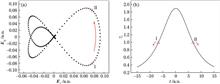
Regulation of Nonadiabaticity-Induced Tunneling Delay Time
Tao Zhou, Mengyao Xu, Sai Zhang, Boqiang Xu, and Sen Cui
Recently, tunneling delay time in attosecond experiments leads to discussions about the nonadiabaticity in tunneling process. Under strong field condition, the tunneling delay time usually can be predicted by Keldysh parameter. However, this prediction will fail when we use a few-cycle orthogonal polarized two-color laser field with an envelope. At this time, the initial momentum of photoelectron and the energy consumed in the tunneling process are two important factors that affect the tunneling delay time. Therefore, we find the relationship between these two factors with ionization probability under the above-mentioned laser field. By changing the field intensity ratio and phase difference of the orthogonal polarized two-color lasers, their influence on the tunneling delay time is identified separately, meanwhile, the regulation of tunneling delay time is achieved. Finally, we find that the energy consumed in the tunneling process is a dominant factor influencing the tunneling delay time. These findings contribute to the quantitative analysis of non-adiabatic tunneling delay time and provide new ideas for regulating the ultrafast non-adiabatic tunneling process. Recently, tunneling delay time in attosecond experiments leads to discussions about the nonadiabaticity in tunneling process. Under strong field condition, the tunneling delay time usually can be predicted by Keldysh parameter. However, this prediction will fail when we use a few-cycle orthogonal polarized two-color laser field with an envelope. At this time, the initial momentum of photoelectron and the energy consumed in the tunneling process are two important factors that affect the tunneling delay time. Therefore, we find the relationship between these two factors with ionization probability under the above-mentioned laser field. By changing the field intensity ratio and phase difference of the orthogonal polarized two-color lasers, their influence on the tunneling delay time is identified separately, meanwhile, the regulation of tunneling delay time is achieved. Finally, we find that the energy consumed in the tunneling process is a dominant factor influencing the tunneling delay time. These findings contribute to the quantitative analysis of non-adiabatic tunneling delay time and provide new ideas for regulating the ultrafast non-adiabatic tunneling process.
Laser & Optoelectronics Progress
- Publication Date: Mar. 10, 2024
- Vol. 61, Issue 5, 0532001 (2024)

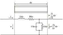
Study on Gain Uniformity of Microchannel Plate
Pokun Deng, Kaixuan Lin, Qiuyan Luo, Jinghua Long, Dong Wang, Yunfei Lei, Junkun Huang, Yong Wang, Houzhi Cai, Jinyuan Liu, and Lihong Niu
When a gated framing camera is operating, the gating pulse transmission attenuation effect will greatly weaken the gain of microchannel plate (MCP) microstrip line and affect the camera performance. The attenuation model of gate voltage pulse transmitting on MCP microstrip line was established, and the gain uniformity of MCP was simulated. As the results, amplitude of voltage pulse decays exponentially in MCP microstrip. Under the attenuation coefficient of 0.0041 Np/mm, the voltage amplitude attenuates to 85% of the original value and the MCP gain attenuates to 29% of the original value at the position of 40 mm. Effects on MCP gain uniformity caused by three methods (voltage compensation, microstrip end reflection compensation, and width gradient microstrip line compensation) were simulated. The three compensation methods were combined to obtain a microstrip line compensation model. In the model, for the minimum width of microstrip is 4 mm, the voltage transmission amplitude is maintained above 94%, and the MCP gain is maintained at 66%. When a gated framing camera is operating, the gating pulse transmission attenuation effect will greatly weaken the gain of microchannel plate (MCP) microstrip line and affect the camera performance. The attenuation model of gate voltage pulse transmitting on MCP microstrip line was established, and the gain uniformity of MCP was simulated. As the results, amplitude of voltage pulse decays exponentially in MCP microstrip. Under the attenuation coefficient of 0.0041 Np/mm, the voltage amplitude attenuates to 85% of the original value and the MCP gain attenuates to 29% of the original value at the position of 40 mm. Effects on MCP gain uniformity caused by three methods (voltage compensation, microstrip end reflection compensation, and width gradient microstrip line compensation) were simulated. The three compensation methods were combined to obtain a microstrip line compensation model. In the model, for the minimum width of microstrip is 4 mm, the voltage transmission amplitude is maintained above 94%, and the MCP gain is maintained at 66%.
Laser & Optoelectronics Progress
- Publication Date: Dec. 10, 2022
- Vol. 59, Issue 23, 2332001 (2022)
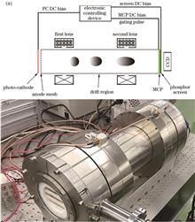
Imaging Performance of Double-Lens Pulse-Dilation Framing Camera
Yunfei Lei, Jinyuan Liu, Houzhi Cai, Junkun Huang, Yong Wang, and Pokun Deng
In this study, a pulse-dilation framing camera using double magnetic lenses to correct aberrations is reported. The spatial resolution, field curvature, and astigmatism characteristics of the camera were analyzed. When the imaging ratio is 2:1, the radius of the working area of the framing camera with a single magnetic lens is 15 mm, and the spatial resolution at a 15-mm off-axis distance is 2 lp/mm. When double magnetic lenses are used in this system, some aberrations are corrected, the radius of the working area is 30 mm, and the spatial resolution at a 15-mm off-axis distance is 5 lp/mm. The field curvature of the camera with a single lens and double lenses was measured and simulated. In a single-lens imaging system, the axial distance between the imaging point at 15-mm off-axis of the field surface and the image point on the axis is around 11 cm, while in a double-lens imaging system, it is about 3 cm. The astigmatism of the double-lens system is analyzed. In the experiment, sagittal and tangential image surfaces are fitted, and the sagittal and tangential resolutions can reach 10 lp/mm. In this study, a pulse-dilation framing camera using double magnetic lenses to correct aberrations is reported. The spatial resolution, field curvature, and astigmatism characteristics of the camera were analyzed. When the imaging ratio is 2:1, the radius of the working area of the framing camera with a single magnetic lens is 15 mm, and the spatial resolution at a 15-mm off-axis distance is 2 lp/mm. When double magnetic lenses are used in this system, some aberrations are corrected, the radius of the working area is 30 mm, and the spatial resolution at a 15-mm off-axis distance is 5 lp/mm. The field curvature of the camera with a single lens and double lenses was measured and simulated. In a single-lens imaging system, the axial distance between the imaging point at 15-mm off-axis of the field surface and the image point on the axis is around 11 cm, while in a double-lens imaging system, it is about 3 cm. The astigmatism of the double-lens system is analyzed. In the experiment, sagittal and tangential image surfaces are fitted, and the sagittal and tangential resolutions can reach 10 lp/mm.
Laser & Optoelectronics Progress
- Publication Date: Sep. 25, 2022
- Vol. 59, Issue 18, 1832001 (2022)
Research on Numerical Simulation of Ultrafast Laser Polishing Brittle Optical Materials
Lü Kexin, and Xuesong Han
In order to analyze the influence of process parameters on the surface polishing results of ultrafast laser polishing hard and brittle optical materials during the polishing process, based on the interaction mechanism of ultrafast laser and hard and brittle dielectric materials, according to the analytical model of the removal function of ultrafast laser polishing dielectric materials, a single-pulse material removal model related to the two processing parameters of defocus and incident angle is established. Using the software and according to the change law of the multi-pulse ablation threshold of dielectric materials, a computational model of ultrafast-laser polishing of hard and brittle optical materials is established, and the results of ultrafast-laser polishing of the material surface under different incident angles and advance lengths are calculated by using the model. This calculation model can directly explain the results of ultrafast laser polishing optical materials, and provide new theoretical guidance for the selection of appropriate laser polishing process parameters and methods. In order to analyze the influence of process parameters on the surface polishing results of ultrafast laser polishing hard and brittle optical materials during the polishing process, based on the interaction mechanism of ultrafast laser and hard and brittle dielectric materials, according to the analytical model of the removal function of ultrafast laser polishing dielectric materials, a single-pulse material removal model related to the two processing parameters of defocus and incident angle is established. Using the software and according to the change law of the multi-pulse ablation threshold of dielectric materials, a computational model of ultrafast-laser polishing of hard and brittle optical materials is established, and the results of ultrafast-laser polishing of the material surface under different incident angles and advance lengths are calculated by using the model. This calculation model can directly explain the results of ultrafast laser polishing optical materials, and provide new theoretical guidance for the selection of appropriate laser polishing process parameters and methods.
Laser & Optoelectronics Progress
- Publication Date: Jan. 01, 2021
- Vol. 58, Issue 5, 0532001 (2021)

Brightness Characteristics and Fractal Dimension of Spot Ablated by Femtosecond Laser
Fubin Wang, and Zhilin Sun
The plasma brightness characteristics derived from the femtosecond laser in the micromachining process can be used as real-time feedback measurement signals. Therefore, it is of great significance to study the brightness characteristics of the spot and construct a high-quality brightness change curve with rich details. In this paper, first, in view of the low signal-to-noise ratio of the spot image and the blurred edge of the target area, the improved wavelet threshold denoising method is used to filter the spot image, and a smooth spot with higher edge contrast can be obtained without changing the brightness level of the spot. Then, the K-means clustering method is used to segment the light spot image, and the halo part that appears as noise is segmented out, and only the area with effective brightness is retained. Finally, the brightness change curve of the light spot sequence image is extracted, and the curve is processed by the method of combining fractal and multi-scale soft threshold filtering, and a high-quality brightness change curve with richly detailed information is obtained. The brightness and fractal dimension are calculated using spot images with different powers. The results show that the brightness of the spot and the complexity of the spot transformation both increase with the increase of the laser processing power. The plasma brightness characteristics derived from the femtosecond laser in the micromachining process can be used as real-time feedback measurement signals. Therefore, it is of great significance to study the brightness characteristics of the spot and construct a high-quality brightness change curve with rich details. In this paper, first, in view of the low signal-to-noise ratio of the spot image and the blurred edge of the target area, the improved wavelet threshold denoising method is used to filter the spot image, and a smooth spot with higher edge contrast can be obtained without changing the brightness level of the spot. Then, the K-means clustering method is used to segment the light spot image, and the halo part that appears as noise is segmented out, and only the area with effective brightness is retained. Finally, the brightness change curve of the light spot sequence image is extracted, and the curve is processed by the method of combining fractal and multi-scale soft threshold filtering, and a high-quality brightness change curve with richly detailed information is obtained. The brightness and fractal dimension are calculated using spot images with different powers. The results show that the brightness of the spot and the complexity of the spot transformation both increase with the increase of the laser processing power.
Laser & Optoelectronics Progress
- Publication Date: Dec. 03, 2021
- Vol. 58, Issue 24, 2432001 (2021)

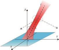
Heavy Ion Single Event Effect Test Calibration System
Haolin Liu, Qing Liu, Xiaohui Zhang, Jing Sun, Song Gu, and Zhengyu Zhong
In response to the need for rapid calibration of the domestic accelerator beam and referring to the single event rollover monitor of European Space Agency, this paper successfully developed a heavy ion single event effect calibration system and successfully applied it to the domestic tandem heavy ion accelerator beam single event test calibration. The test results show that 11 kinds of heavy ions can be calibrated to the SEU (Single Event Upset) cross-section data of the system in the "00" and "FF" data modes under the irradiation angles of 0°, 45° and 60°, respectively. By comparing with the results of single-event flipping test data of major accelerators at home and abroad, the physical distribution of single-event flipping inside the calibration system is analyzed, which verifies that the designed single-particle calibration system can accurately monitor the accuracy and uniformity of the heavy ion accelerator beam. In response to the need for rapid calibration of the domestic accelerator beam and referring to the single event rollover monitor of European Space Agency, this paper successfully developed a heavy ion single event effect calibration system and successfully applied it to the domestic tandem heavy ion accelerator beam single event test calibration. The test results show that 11 kinds of heavy ions can be calibrated to the SEU (Single Event Upset) cross-section data of the system in the "00" and "FF" data modes under the irradiation angles of 0°, 45° and 60°, respectively. By comparing with the results of single-event flipping test data of major accelerators at home and abroad, the physical distribution of single-event flipping inside the calibration system is analyzed, which verifies that the designed single-particle calibration system can accurately monitor the accuracy and uniformity of the heavy ion accelerator beam.
Laser & Optoelectronics Progress
- Publication Date: Sep. 10, 2021
- Vol. 58, Issue 17, 1732001 (2021)
Chirped Pulse Compression Based on Fresnel-Inspired Binary Phase Shaping
Baihong Li, Zhiguang Xia, Pengda Zhao, Xiao Xiang, Ruifang Dong, and Tao Zhang
Phase compensation is one of the key technologies for pulse compression and ultrashort laser pulse generation. First, we use the phase function of the Fresnel binary phase shaping scheme can achieve a lens-like function, and can introduce a negative secondary spectral phase (negative dispersion) in the frequency domain. Then, the proposed scheme is used to compensate the dispersion of the chirped pulse, thereby turning it into a transformed-limited pulse, and its pulse width is compressed to the time width of the transformed-limited. The proposed scheme is only related to the quadratic phase and does not depend on the spectral amplitude, so it is applicable to various pulse shapes with symmetrical distribution. Finally, the numerical calculation results of common Gaussian pulse and square-wave pulse are given to verify the correctness of the proposed scheme in theory. The proposed scheme provides a new idea and method for chirped pulse compression, and can be extended to other fields related to dispersion compensation. Phase compensation is one of the key technologies for pulse compression and ultrashort laser pulse generation. First, we use the phase function of the Fresnel binary phase shaping scheme can achieve a lens-like function, and can introduce a negative secondary spectral phase (negative dispersion) in the frequency domain. Then, the proposed scheme is used to compensate the dispersion of the chirped pulse, thereby turning it into a transformed-limited pulse, and its pulse width is compressed to the time width of the transformed-limited. The proposed scheme is only related to the quadratic phase and does not depend on the spectral amplitude, so it is applicable to various pulse shapes with symmetrical distribution. Finally, the numerical calculation results of common Gaussian pulse and square-wave pulse are given to verify the correctness of the proposed scheme in theory. The proposed scheme provides a new idea and method for chirped pulse compression, and can be extended to other fields related to dispersion compensation.
Laser & Optoelectronics Progress
- Publication Date: Sep. 30, 2020
- Vol. 57, Issue 19, 193201 (2020)
Wavelet Processing and Analysis of Grayscale Features of Femtosecond Laser Ablation Spots
Fubin Wang, Zhilin Sun, and Shangzheng Wang
In this study, the grayscale characteristics of plasma spots are analyzed. First, the L component of the original spot images is extracted based on the principal component combined with mask processing in the HSL color space. Thus, effective grayscale images can be obtained with a high signal-to-noise ratio. The average grayscale curves of single spot image are analyzed before and after processing, and the grayscale curves of the original spot images contain several burrs, whereas those of the processed image are smoother. Second, by extracting the grayscale feature of the spot sequence images, the graysale value of the spot sequence images can be observed to change periodically with the reciprocating ablation motion of the femtosecond laser beam. Third, a method that combines fractal interpolation with wavelet transformation is used for processing the average grayscale characteristic curves of the spot sequence images. This method not only keeps the detail information of the average grayscale characteristic curve clearly, but also makes the curve smoother. Finally, by analyzing the correlation between the spot grayscale characteristics as well as the ablative processing power and the movement of the processing platform, a strong correlation can be observed between them. Thus, this study provides a significant basis for adjusting the laser power and obtaining the processing-depth feedback of microstructures based on the spot grayscale index. In this study, the grayscale characteristics of plasma spots are analyzed. First, the L component of the original spot images is extracted based on the principal component combined with mask processing in the HSL color space. Thus, effective grayscale images can be obtained with a high signal-to-noise ratio. The average grayscale curves of single spot image are analyzed before and after processing, and the grayscale curves of the original spot images contain several burrs, whereas those of the processed image are smoother. Second, by extracting the grayscale feature of the spot sequence images, the graysale value of the spot sequence images can be observed to change periodically with the reciprocating ablation motion of the femtosecond laser beam. Third, a method that combines fractal interpolation with wavelet transformation is used for processing the average grayscale characteristic curves of the spot sequence images. This method not only keeps the detail information of the average grayscale characteristic curve clearly, but also makes the curve smoother. Finally, by analyzing the correlation between the spot grayscale characteristics as well as the ablative processing power and the movement of the processing platform, a strong correlation can be observed between them. Thus, this study provides a significant basis for adjusting the laser power and obtaining the processing-depth feedback of microstructures based on the spot grayscale index.
Laser & Optoelectronics Progress
- Publication Date: Sep. 02, 2020
- Vol. 57, Issue 18, 183201 (2020)
Ultrafast Carrier Dynamics in n-Type and Semi-Insulating 6H-SiC Crystals
Yao Nie, Youyun Wang, Xueqin Wu, and Yu Fang
The ultrafast transient absorption spectroscopy of interband excitation is utilized to evaluate the ultrafast carrier recombination dynamics in the conductive (n-type) nitrogen (N)-doped and semi-insulating (SI) vanadium (V)-doped 6H-SiC wafers. The carrier relaxation of n-type 6H-SiC with carrier lifetime more than 10 ns is dominated by indirect recombination through N impurities and/or inherent defects. Compared with the n-type 6H-SiC, the V-doped one has a pronounced modulation of transient absorption, resulting from an additional carrier recombination process caused by the carrier trapping of V deep levels. The carrier-trapping with a lifetime of about 160 ps is more than two orders of magnitude faster than the indirect recombination. With a simplified energy level model and the global analysis, the carrier recombination mechanism is investigated and the carrier lifetime of 6H-SiC is determined accurately. The ultrafast transient absorption spectroscopy of interband excitation is utilized to evaluate the ultrafast carrier recombination dynamics in the conductive (n-type) nitrogen (N)-doped and semi-insulating (SI) vanadium (V)-doped 6H-SiC wafers. The carrier relaxation of n-type 6H-SiC with carrier lifetime more than 10 ns is dominated by indirect recombination through N impurities and/or inherent defects. Compared with the n-type 6H-SiC, the V-doped one has a pronounced modulation of transient absorption, resulting from an additional carrier recombination process caused by the carrier trapping of V deep levels. The carrier-trapping with a lifetime of about 160 ps is more than two orders of magnitude faster than the indirect recombination. With a simplified energy level model and the global analysis, the carrier recombination mechanism is investigated and the carrier lifetime of 6H-SiC is determined accurately.
Laser & Optoelectronics Progress
- Publication Date: Mar. 14, 2019
- Vol. 56, Issue 6, 063201 (2019)
Fabrication of Silicon Micro/Nanostructures Based on Laser Interference Ablation
Zihan Wang, Baoxu Wang, Masaru Kamano, and Weiwei Xu
Based on nanosecond laser two-beam interference ablation assisted with wet-etching method and finite difference time domain (FDTD) simulation, the formation of structures on silicon is studied experimentally and theoretically. The results show that it is possible for the fabrication of structures with period more than 600 nm by a nanosecond laser with wavelength of 355 nm. The structure depth becomes deeper with the increasing of power or exposure time. The maximum depth is equal to the skin depth of laser, about 50 nm. Further, the period splits into half when the exposure time is more than 5 s, which brings a method to obtain a minimum period of 300 nm. The FDTD simulation confirms that the modulation of formed structures to the interference field is the reason for period splitting. The research shows great potential applications for the fabrication of periodic micro/nanostructures, design of maskless processing facilities, and laser-matter interactions. Based on nanosecond laser two-beam interference ablation assisted with wet-etching method and finite difference time domain (FDTD) simulation, the formation of structures on silicon is studied experimentally and theoretically. The results show that it is possible for the fabrication of structures with period more than 600 nm by a nanosecond laser with wavelength of 355 nm. The structure depth becomes deeper with the increasing of power or exposure time. The maximum depth is equal to the skin depth of laser, about 50 nm. Further, the period splits into half when the exposure time is more than 5 s, which brings a method to obtain a minimum period of 300 nm. The FDTD simulation confirms that the modulation of formed structures to the interference field is the reason for period splitting. The research shows great potential applications for the fabrication of periodic micro/nanostructures, design of maskless processing facilities, and laser-matter interactions.
Laser & Optoelectronics Progress
- Publication Date: Aug. 04, 2019
- Vol. 56, Issue 16, 163201 (2019)
Topics
© Copyright 2018-2021 | Chinese Laser Press. All Rights Reserved 沪ICP备15018463号-20